고정 헤더 영역
상세 컨텐츠
본문
Serial Peripheral Interface – SPI Basics Hey all! It’s time to continue with our tutorials on serial communication. Till now, we have covered the following:. Apart from this, there are few other serial transfer protocols like SPI, I2C, etc. In this post, we will discuss about SPI and its bus transactions – no programming, just the concepts. Programming the SPI of (AVR) microcontrollers will be discussed in upcoming post. Contents.
- Serial Peripheral Interface Tutorial
- Motorola Serial Peripheral Interface Specification Download
- Serial Peripheral Interface Specification

Serial Peripheral Interface (SPI) Serial Peripheral Interface, often shortened as SPI (pronounced as spy, or ess-pee-eye), is a synchronous serial data transfer protocol named by Motorola. Here two or more serial devices are connected to each other in. The devices connected to each other are either Master or Slave. In a SPI link there could as many Masters and Slaves as required, but it’s very rare to find more than one Master in a SPI link. The Master device is the one which initiates the connection and controls it. Once the connection is initiated, then the Master and one or more Slave(s) can transmit and/or receive data. As mentioned earlier, this is a full-duplex connection, which means that Master can send data to Slave(s) and the Slave(s) can also send the data to the Master at the same time.
Serial Peripheral Interface Tutorial
SPI Bus Transaction Now that we have a basic knowledge of what SPI is, let’s look into the operation of SPI Bus. The SPI operation is based upon shift registers. Every device, whether Master or Slave has an 8-bit shift register inside it. The size of the shift register could be more than 8-bit as well (like 10-bit, 12-bit, etc), but it should be the same for both Master and Slave, and the protocol should support it. Hardware Setup The Master and Slave are connected in such a way that the two shift registers form an inter-device circular buffer. The following diagram should explains the hardware setup. Please click on the images to enlarge it and view it in high resolution.
Hardware Setup of Master-Slave Device and Shift Registers (Click to Enlarge) As you can see, there is an 8-bit shift register inside each of the Master and Slave devices. These shift registers operate in fashion. The output of the Master’s shift register is connected to the input of the Slave’s shift register; and the output of the Slave’s shift register is connected to the input of Master’s shift register.
This makes the connection operate like a circular/ring buffer. Don’t bother about the names MISO, MOSI and SCK now. We will discuss about them a little later in this post.
As mentioned earlier, SPI is a synchronous serial data transfer protocol, which means that there must be a clock to synchronize the data transfer. It has also been stated that the Master is responsible for initiating and controlling the connection. Thus, we use the clock source of the Master device to synchronize the data transfer.
That’s why you see the clock source inside the Master, which controls the operation of both the shift registers. Data Transfer Operation Alright, now let’s see how SPI bus transfers data among Master and Slave. Let’s refer to the diagram shown in the above section. Let’s say that the data in the Master’s shift register is A7 through A0 (MSB through LSB) whereas the data in the Slave’s shift register is B7 through B0 (MSB through LSB). This is the initial state before any clock pulse arrives.
Now as soon as a clock pulse arrives, the shift registers come into operation and the data in the registers in shifted by one bit towards the right. This evicts bit A0 from Master and bit B0 from Slave. Since the Master and Slave are connected to form a ring/circular buffer, the evicted bit occupies the MSB position of the other device. Which means, bit A0 gets evicted from Master and occupies MSB position in Slave’s shift register; whereas bit B0 gets evicted from Slave and occupies MSB position in Master’s shift register. This can be seen in the following image. Bits are color coded for better viewing.
Please click on the image to enlarge it. Clock Pulse 8 – SPI Bus Transaction showing Master Slave Shift Registers (Click to Enlarge) And here’s an animation.
Thanks to for creating it! Short Summary To sum up,. Both, Master and Slave place the data (byte) they wish to transfer in their respective shift registers before the communication starts.

Master generates 8 clock pulses. After each clock pulse, one bit of information is transfer from Master to Slave and vice-versa.
After 8 clock pulses, Master would have received Slave’s data, whereas Slave would have Master’s data. And that’s why this is a full-duplex communication. SPI Bus Interface Now that we are conceptually clear how the data transfer takes place, let’s look into the SBI bus description and the interface between Master and Slave. The Master and Slave are connected by means of four wires. Each of these wires carries a particular signal defined by the SPI bus protocol.
These four signals/wires are–. MOSI – Master Out Slave In: This is the wire/signal which goes from the output of Master’s shift register to the input of the Slave’s shift register.
MISO – Master In Slave Out: This is the wire/signal which goes from the output of Slave’s shift register to the input of the Master’s shift register. SCK/SCLK – Serial Clock: This is the output of the clock generator for Master and clock input for Slave. SS’ – Slave Select: This is discussed in the next section of this post. The MOSI, SCK and SS’ signals are directed from Master to Slave whereas the MISO signal is directed from Slave to Master.
The following diagram represents this interface having single Master and single Slave. SPI Bus – Single Master Single Slave (Click to Enlarge) Thus, it should be noted again that during each SPI clock cycle, a full duplex transmission occurs as follows–. Master sends a bit to the MOSI line; Slave reads it from the same line.
Motorola Serial Peripheral Interface Specification Download
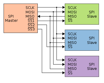
Slave sends a bit to the MISO line; Master reads it from the same line. Multiple Slaves – Slave Select (SS’) Signal As mentioned earlier, SPI can be used to connect one Master to multiple Slaves as well. Having multiple Masters is also possible, but it does nothing but increase the complexity due to clock synchronization issues, and is very very rare. Having multiple Slaves is where the Slave Select (SS’) signal comes into effect. SS’ (which means SS complemented) signal is in active low configuration i.e. To select a particular Slave, we need to provide a LOW signal level to SS’ of the Slave. The SPI bus interface is pretty simple for this one, and is shown in the diagram shown below.
SPI Bus – Single Master Multiple Slaves (Click to Enlarge) All the Slaves share the same MOSI, MISO and SCK signals. The SS’ signal is responsible for choosing a particular Slave. The Slave gets enabled only when its input SS’ signal goes LOW.
In the above case, each of the Slaves is independent since they are separately selected via independent SS’ signals from the Master. However, there is another way to link the Slaves together – by using. In this configuration, all the Slaves are selected at a time, and the output of one Slave goes to the input of another Slave, and so on. However we will not be discussing this here (and in upcoming posts as well) since most of the applications don’t require this type of configuration.
Clock Polarity and Phase Keeping synchronization in mind, Master’s role doesn’t end with simply generating clock pulses at a particular frequency (usually within the range of 10 kHz to 100 MHz). In fact, Master and Slave should agree on a particular synchronization protocol as well, or else everything will go wrong and data will get lost. This is where the concept of clock polarity (CPOL) and clock phase (CPHA) comes in. CPOL – Clock Polarity: This determines the base value of the clock i.e.
Serial Peripheral Interface Specification
The value of the clock when SPI bus is idle. When CPOL = 0, base value of clock is zero i.e.
SCK is LOW when idle. When CPOL = 1, base value of clock is one i.e.

SCK is HIGH when idle. CPHA – Clock Phase: This determines the clock transition at which data will be sampled/captured. When CPHA = 0, data is sampled at clock’s rising/leading edge. When CPHA = 1, data is sampled at clock’s falling/trailing edge. This results in four SPI modes, shown in the table below taken from the page 139.
We will discuss more about these modes and how to choose them in our next post where we will learn how to program the SPI of the AVR. Connections between ISP and AVR MCU (Click to Enlarge) This means that if you have connected some SPI device to your AVR microcontroller, and at the same time you are trying to program your microcontroller, there could be some issues (like driver contention). We will discuss about this issue and other hardware considerations in our next post. Interesting Reads You might be interested in reading the following documents–. Summary Let’s look at what we have learnt in this post. SPI is a full-duplex synchronous serial data transfer protocol.
Data transfer takes place in between Master and Slave devices. Each Master/Slave device has an internal 8 bit shift register, which is connected to other devices so as to form a circular/ring buffer. At each clock pulse, data gets right shifted in the circular/ring buffer. After 8 clock pulses, data is completely exchanged in between devices. SPI bus consists of four wires/signals – MOSI, MISO, SCK and SS’. When we connect more than one Slave devices, then we choose them using the SS’ signal.
CPOL and CPHA must be set so that Master and Slave devices sync properly. AVR ISP uses SPI to program the microcontroller. So this was all about the basics of SPI. If you want to know about the pros and cons of SPI, I would suggest you to read Wikipedia section.
In the next post, we will learn how to implement SPI in an AVR microcontroller. So subscribe to stay updated! And don’t forget to write your views about this post below. And it’s about to be Thanksgiving time in two weeks, so Happy “early” Thanksgiving!:) Next Post: SPI of AVR Don’t forget to check out the where we show how you can implement SPI using AVR microcontrollers. References. Written By– Mayank Prasad (aka Max) Arizona State University max@maxEmbedded.com Last updated on February 9, 2016.


